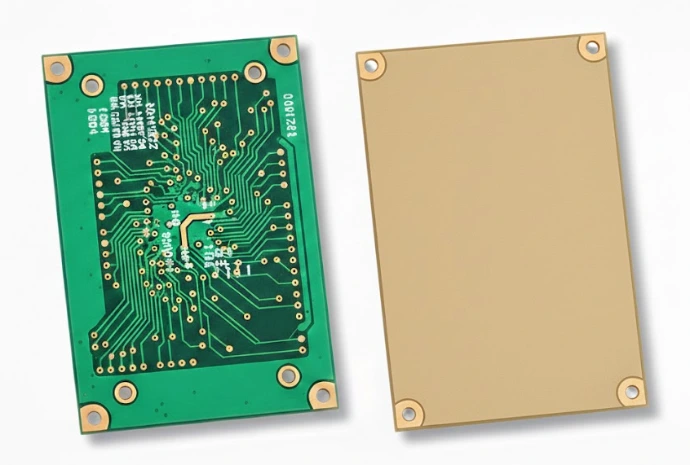
PCB 1/0 (1 PHASE)
Material base: FR4 TG130 KB
Dimensions: Max. 120cm x 35cm, Min. 1cm x 1cm
Quantity: Min. 1 unit, Max. 100 thousand units.
PCB Thickness: 1.6 mm, 1.2 mm, 0.8 mm, 0.5 mm
Solder Mask: Green, red, black, blue, white
Silkscreen (symbols and letters): black and white
Surface finish: HASL (Sn/Pb), ENIG (gold), Gold
Copper thickness: 1 oz, 2 oz.
Single Layer Printed Circuits (1/0) in FR4 and FR1
At Microcircuitos S.A.S.we manufacturesingle layer PCBs (1/0)designed to meet the requirements of the modern electronics industry, combiningtechnical precision, operational reliability, and cost efficiency.
Our boards are developed underindustrial standards, ensuring stable performance during assembly processes and throughout the life of the final product.
1. Thermal performance and solder resistance
Microcircuitos single layer PCBs are prepared to withstand the demanding thermal conditions of production:
High thermal stability
Optimized adhesion between copper and substrate reduces the risk of delamination and lifting of traces, even after multiple soldering and rework cycles.
Compatibility with assembly processes
They can withstand temperatures of up to320 °C, making them suitable for:
Manual assembly with soldering iron
Wave Soldering
2. Versatilidad de Materiales: FR1 vs. FR4
We offer different substrates to optimize technical performance and manufacturing costs.
FR1 – Phenolic substrate (reinforced paper)
Cost-efficient solutionfor volume production and functional prototypes.
Excellent machinability, ideal for punching and drilling, reducing process times and tool wear.
Typical applications: consumer electronics, products with low to medium mechanical stress.
FR4 – Epoxy resin reinforced with fiberglass
Industrial standardwith high mechanical rigidity and impact resistance.
Low moisture absorptionand excellent dielectric properties, ensuring electrical stability in demanding environments.
Recommended for industrial applications and products with higher technical requirements.
3. Customization of copper thickness
We adjust the thickness of the copper layer according to the electrical needs of the design:
1 oz (35 µm)
Standard thickness for control circuits, signals, logic, and general applications.
2 oz (70 µm)
Option for high currents, improves thermal dissipation and reduces electrical losses. Ideal for power tracks and thermal planes.
4. Aplicaciones e Industrias Clave
Single-layer PCBs from Microcircuitos are widely used in:
Power supplies and converters
LED lighting systems
Industrial equipment and controllers
Power drivers and electronic modules
✔ Why manufacture your single-layer PCBs with Microcircuitos?
Local manufacturing withindustrial quality control
Technical support during design and production
Flexible material and copper options
Compliance with manual and industrial assembly processes
👉 Cotice su PCB de una cara FR4 (1/0) con nuestro equipo técnico